NOT Gate with NPN transistors

Overview
Overview
Keywords: Transistor logic, NPN, resistors, LED, Inverter, Boolean algebra, gate, NOT
Age group: 14-17
Required knowledge/skills: Basic electronics, circuit design, working in tinkercad.com virtual environment
Time frame: 1-2 hours: assembling the circuit in Tinkercad
Authors: Astrinos Tsoutsoudakis (GR)

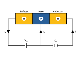
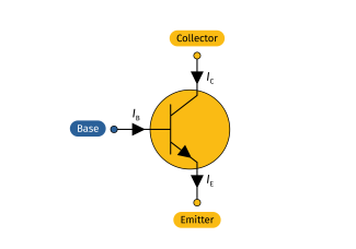
The NPN transistor acts like an electronic switch controlled by the voltage at its base. The circuit typically consists of a power source, a current-limiting resistor for the base, the NPN transistor itself, and a load (like an LED with a resistor) connected to the collector. The emitter is connected to ground.
Input is LOW
When a LOW voltage (or 0V) is applied to the base of the transistor, no significant current flows from the base to the emitter. This effectively keeps the transistor "off," or in its cutoff state. Since the transistor is an open circuit between the collector and emitter, the current cannot flow from the power source through the load to the ground. This causes the full voltage to drop across the load, making the output HIGH.
Input is HIGH
When a HIGH voltage (e.g. 5V) is applied to the base, a small current flows from the base to the emitter, "turning on" the transistor. The transistor then acts as a short circuit between the collector and emitter, putting it in a state of saturation. This allows a large current to flow from the power source, through the load, and to the ground. Since the transistor now has a very low resistance, almost all the voltage from the power supply drops across the load. This causes the output voltage, measured at the collector, to be very close to ground, which is considered LOW.
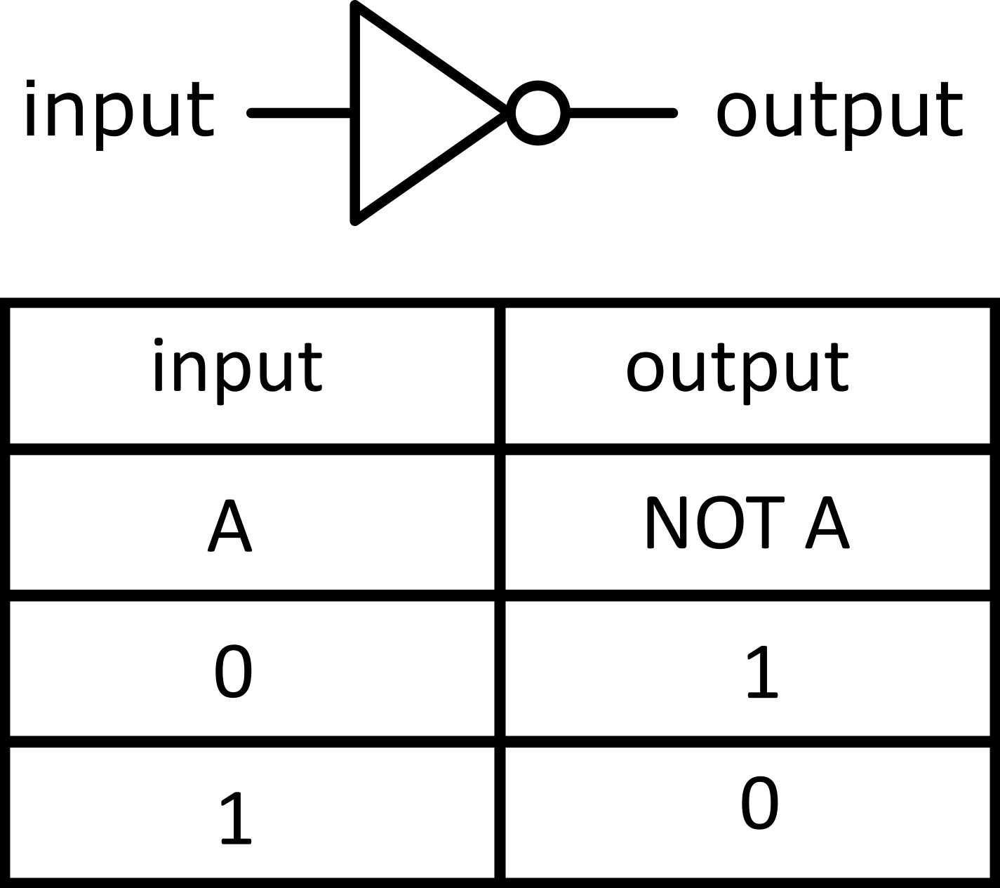
A NOT gate, or inverter, inverts a single digital input – it flips it. If the input is ON, the output is OFF, and if the input is OFF, the output is ON. We're going to build this basic logic gate using an NPN transistor, which acts like an electronic switch.
NPN transistor circuit
NPN transistor symbol
Required materials
- Software: Arduino IDE
- Online tool: tinkercad.com
Hardware
| Name | Quantity | Component |
|---|---|---|
| Bat1 | 1 | 4 AA Batteries 1.5 C |
| S1 | 1 | Pushbutton |
| R1/R3 | 2 | 2 kΩ Resistor |
| T1 | 1 | NPN Transistor (BJT) |
| D1 | 1 | Blue LED |
Tasks for teachers
- Set up Tinkercad classrooms, provide Arduino code templates, circuit diagrams.
- Introduce binary arithmetic (Introduction to Binary) and logic gates (Introduction to Logic Gates).
- Help students place components correctly: transistors, resistors, switches, LEDs.
- Encourage inquiry and discussion.
- Use short quizzes, discussion, or mini presentations to check comprehension.
Tasks for students
- Learn basic electronics.
- Assemble the the circuit in Tinkercad.
- Document the project and present findings.
- Think creatively about how to suggest improvements.
The circuit realized in tinkercad.com virtual environment
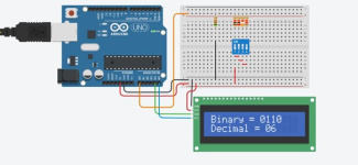
The circuit realized in tinkercad.com virtual environment
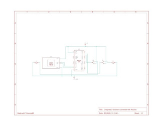
Schematics of the circuit
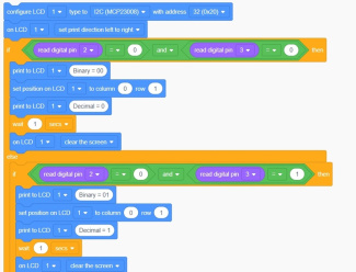
Part of the Code in Blocks
You can find the circuit in Tinkercad to reuse here.
Share this page